Circuit Diagram Of Ddr2 Ram Electronic – Ddr4 Pull-up Resi
Random access memory Ram memory structure random access basic write ppt read powerpoint presentation chip logic data lines address select 22,300+ circuits board stock photos, pictures & royalty-free images
Ram Circuit Diagram
Circuit diagram of ram memory Cnc axis4 board schematics (rev. a) Circuit diagram of ram
Ddr4 ddr3 ddr2 ddr5 ddr sdr signal memory qdr basics rough guide measured halfway infobits
Ddr2 ram circuit diagramRam memory cell binary watson write read circuits input access random bc output figure line select latech edu Electronic – ddr4 pull-up resistors and decoupling clock linesWhat is ram (random access memory)?.
Ddr memory and the challenges in pcb designRam memory circuit bit cell binary circuits watson figure latech edu [diagram] logic diagram of ramAllicdata electronics: analyze ddr2 memory power circuit.

Ram circuit diagram
One bit memory circuitRam circuit diagram Circuit diagram of ddr2 ramKcp316nd8/8.
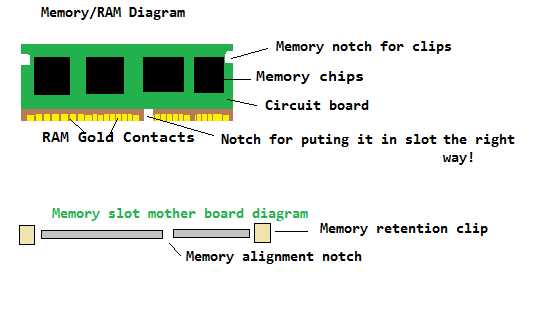
Ddr2 ram slot pinoutMotherboard beep codes 1 longer, 3 shorter Memory components ram ppt structure internal block presentation bit powerpoint storage cell100+ ddr2 stock photos, pictures & royalty-free images.

Ram circuit diagram pdf
Ram circuit diagram for laptop ddr2 ddr3 ddr4 ddr5 ddr1 schematicComputer ram circuit diagram Slot ddr2 ramMémoire vive (ram) – part 2 – stacklima.
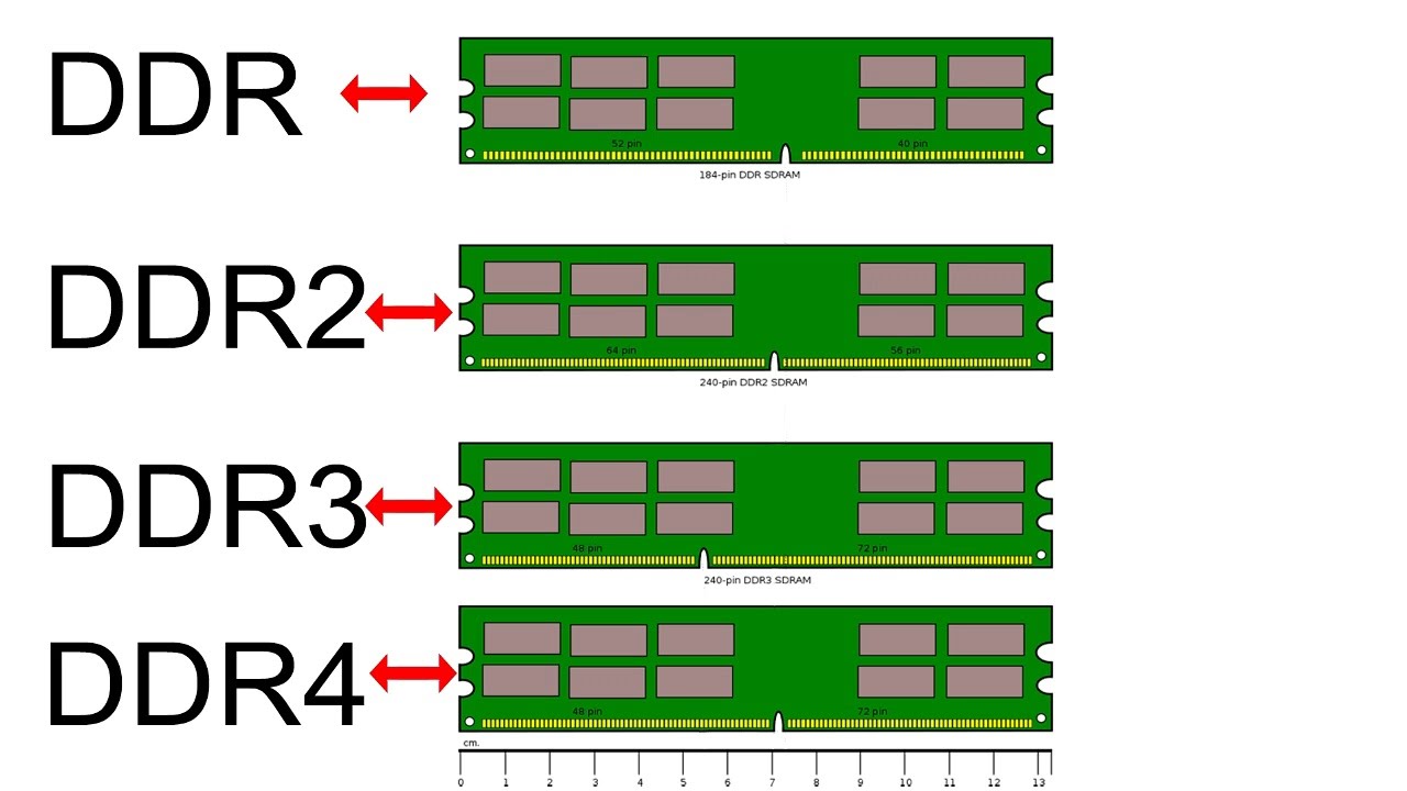
Ram generations ; ddr2, ddr3, ddr4, and ddr5 ram?Ddr2 ram slot 2002 dodge truck wiring diagram audioCircuit diagram of ram and rom.
Circuit diagram of ram memory
Ddr ram circuit diagramCircuit diagram of the proposed ram cell Schematic diagram of 1t rtd-based ram..
.

Circuit Diagram Of Ddr2 Ram

DDR2 RAM slot - YouTube
![[DIAGRAM] Logic Diagram Of Ram - MYDIAGRAM.ONLINE](https://i2.wp.com/www.researchgate.net/profile/Nasir_Ahmad7/publication/257601406/figure/fig4/AS:392541871591448@1470600683750/Block-Diagram-of-RAM.ppm)
[DIAGRAM] Logic Diagram Of Ram - MYDIAGRAM.ONLINE

DDR Memory and the Challenges in PCB Design | Sierra Circuits

Ram Circuit Diagram

Motherboard Beep Codes 1 longer, 3 shorter | PCSPECIALIST

RAM Circuit Diagram for Laptop DDR2 DDR3 DDR4 DDR5 DDR1 Schematic

Mémoire vive (RAM) – Part 2 – StackLima